MILŁPRFŁ50884F
APPENDIX A
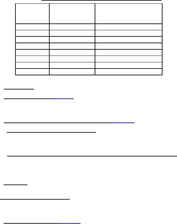
TABLE AŁIII. Thickness of conductors without copper plating (after processing).
Minimum surface conductor
Starting copper
Processing reduction
thickness (after processing)
foil weight
allowance
Inches (μm)
inches (μm)
1/8
.00006 (1.5)
.00012 (3.048)
1/4
.00006 (1.5)
.00024 (6.096)
3/8
.00006 (1.5)
.00037 (9.398)
1/2
.00016 (4.0)
.00045 (11.43)
1
.00024 (6.0)
.00098 (24.892)
2
.00024 (6.0)
.00219 (55.6)
3
.00024 (6.0)
.00341 (86.6)
4
.00024 (6.0)
.00463 (117.6))
A.3.6.2.3 Conductor width. The conductor width shall be as specified (see A.3.1.1).
A.3.6.2.4 Annular ring, internal (see figure GŁ6). The minimum annular ring for functional internal lands on types 3
and 4 printed wiring boards shall be as specified (see A.3.1.1). If not specified on the applicable master drawing, the
minimum internal annular ring should not be less than the values specified in the IPC's 2220 series of documents for
the design of flexible or rigid-flex printed wiring boards.
A.3.6.2.5 Bonding of conductor to base material and lifted lands (see figure GŁ7).
A.3.6.2.5.1 Non-stressed specimens (as received condition). There shall be no lifted lands, or evidence of lifted
lands on the non-stressed microsectioned test specimen. When inspected in accordance with A.4.8.2 and lifted lands
are present, the lot shall be 100 percent visually inspected in accordance with A.4.8.1 for separation of the lands from
the base material.
A.3.6.2.5.2 Stressed specimens (after rework simulation, resistance to soldering heat, or thermal shock). After
undergoing rework simulation, resistance to soldering heat, or thermal shock testing (see A.3.7.4.8, A.3.7.6.2, and
A.3.7.6.3), the maximum allowed distance from the base material surface to the bottom of the edge of the land or pad
shall be no greater than the total land thickness. The total land thickness is equal to the combined thickness of the
metal foil and copper plating on that land.
A.3.6.2.6 Undercutting. Undercutting at each edge of the conductors shall not exceed the total thickness of the
copper foil and plated copper.
A.3.6.3 Hole preparation prior to metallization. The presence of both flexible and rigid base materials in type 4
designs will cause varying degrees of etchback amongst the various base materials in the finished plated-through
hole. In addition, all designs that make use of adhesiveless flexible base material will typically exhibit minimal
etchback at the flexible dielectric to copper conductor interface.
A.3.6.3.1 Desmear (hole cleaning) (see figure GŁ8). When etchback is not specified on the applicable master
drawing, the vertical faces of the internal conductors of holes that will be plated shall be cleaned to be free of resin
smear. Lateral removal of base material from the hole wall shall not exceed .001 inch (0.03 mm). When desmear is
used for hole preparation, a negative etchback of .0005 inch (0.013 mm) maximum shall be acceptable.
27
For Parts Inquires submit RFQ to Parts Hangar, Inc.
© Copyright 2015 Integrated Publishing, Inc.
A Service Disabled Veteran Owned Small Business