MIL-DTL-62737A(AT)
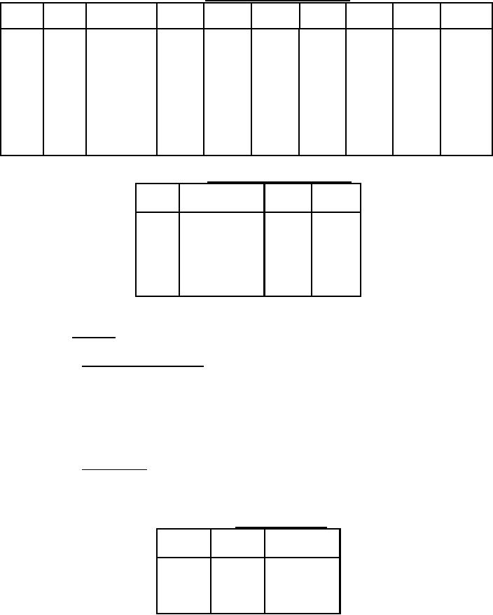
TABLE VI. Memory chip select logic levels.
U10 pin
U26-15
U26-14
U26-13
U26-12
U26-10
U26-9
U26-7
U25-5
U33-5
19 16 15
U2-20
U3-20
U8-20
U4-20
U5-20
U6-20
U7-20
X
0
X X
X
1
1
1
1
1
1
1
1
X
X X
X
1
1
1
1
1
1
1
0
1
0
0
0
0
1
1
1
1
1
1
0
1
0
0
1
1
0
1
1
1
1
1
0
1
0
1
0
1
1
0
1
1
1
1
0
1
0
1
1
1
1
1
0
1
1
1
0
1
1
0
0
1
1
1
1
1
1
1
0
1
1
0
1
1
1
1
1
0
1
1
0
1
1
1
0
1
1
1
1
1
0
1
0
1
1
1
1
1
1
1
1
1
1
0
TABLE VII. Memory chip select logic levels.
U10 pin
U27-15 U27-13
U25-5 15 16 19 U9-20
U8-20
0
X
X
X
1
1
1
0
0
0
0
1
1
0
0
1
1
1
1
0
1
0
1
0
1
0
1
1
1
1
1
1
X
X
1
1
(X denotes a don't care conditions)
3.3.8 Memory.
3.3.8.1 Bootstrap EPROM read. U9 pins 11 through 13, and 15 through 19 shall drive
the data BUS with logic levels defined by the logic levels present at U9 pins 1 through 10, 21, and
24 through 27, (see 6.3) when the control signals (MRD/ - U19-14, and EPS/ - U27-15) conform
to the waveforms in figure 5. Logic levels at U9 pins 26 and 27 are determined by logic levels at
CNTR1 (U24-5) and CNTR2 (U24-9), respectively. See table VIII for the address range for each
control line setting.
3.3.8.2 SRAM write. U8 shall store the logic levels present at U1 pins 8 through 15 in a
location defined by the logic levels present at U8 pins 2 through 10, 21, and 23 through 25 when
the control signals (MWR/ - U20-17 and RS/ - U32-6) conform to the waveform in figure 6.
TABLE VIII. EPROM addressing.
CNTR1 CNTR2
U9 address
U24-5
U24-9
range (Hex)
0
0
0000 - 1FFF
1
2000 - 3FFF
0
1
0
4000 - 5FFF
1
1
6000 - 7FFF
9
For Parts Inquires submit RFQ to Parts Hangar, Inc.
© Copyright 2015 Integrated Publishing, Inc.
A Service Disabled Veteran Owned Small Business